solar cells,solar cell,antireflection coating,antireflection coatings,antireflection,selective emitter,emitter,surface oxide texturing,surface texturing,texturing,CVD,passivation,passivating,efficiency,low sheet resistance,shunt resistance,process,technique,RTWCG,chemical,growth,c-Si,mc-Si,Si


The Specmat RTWCG Technology

The Room Temperature Wet 
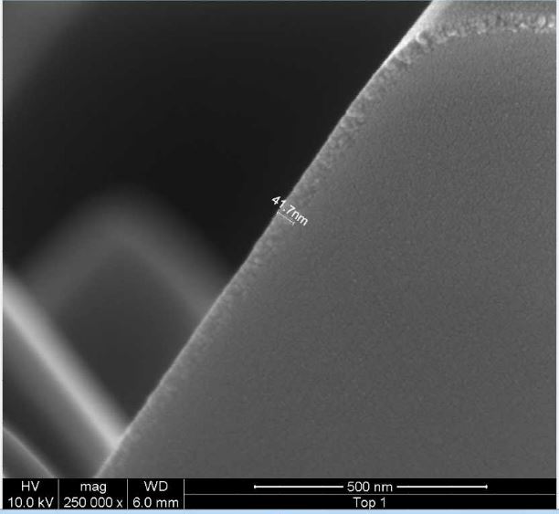
Chemistry Growth (RTWCG) technology is a novel technology for growing highly uniform amorphous SiOx layers into silicon substrates. It can be broken down 
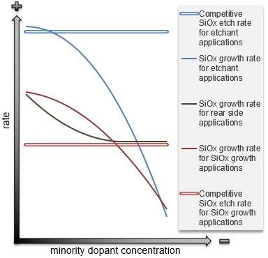
into two kinds of applications: as a chemical etchant and as a SiOx growth chemistry.

oxide etch rate oxide growth rateFor etching applications, see the chart to the left, the RTWCG formulation is adjusted to maximize the competitive SiOx etch rate (double blue line) so that it exceeds the oxide growth rate (blue line). For SiOx growth applications, the RTWCG formulation’s SiOx growth rate (red line) is optimized to exceed the competitive oxide etch rate (double red line).  By varying the SiOx growth rate and/or the competitive oxide etch rate, RTWCG SiOx growth solutions can be formulated to create SiOx thicknesses that range from no oxide to up to 5,000 Angstrom (Å) per a certain constant substrate etch-back.

In PV, the RTWCG etch technology can be utilized in various ways such as:  dead layer etching, surface etching for selective emitter applications, and as a junction isolation process. The SiOx growth technology can be used to improve the optical properties of solar cells, to mitigate PID, and to increase passivation when used in, for instance, a SiNx/SiOx stack.  Additionally, the oxide can be grown to a sufficient thickness to be used in applications that require the use of a mask or even an antireflection coating.

oxide growth on textured silicon wafer pyramidThe SEM image on the left shows a 400Å-thick RTWCG SiOx oxide layer which was grown in 60 seconds on a textured single-crystalline silicon wafer.  The SiOx layer is made up of silicon (Si), oxygen (O), and x can be either fluorine (F), carbon (C), nitrogen (N), oxygen (O), or some other element depending on the redox system being used.  The SiOx growth process can be precisely controlled to accurately create specific thicknesses at specific growth rates.  The thickness range can be from 0Å to 5,000Å and the growth rate can range from as high as 100Å per second to 100Å per hour.

For the photovoltaic (PV) industry, the technology can be applied to, either or both, the front and rear side of the solar cell to yield the following:

o    Front side silicon nitride (SiNx)/SiOx passivation and anti-reflection stack;

o    Front side SiOx passivation and anti-reflection coating (ARC);

o    Rear side parasitic emitter etch for junction isolation;

o    Rear side SiOx passivation layer growth;

o    Rear side SiOx optical layer;

o    Diffusion barrier layer.

The following cell architectures for both N-type and P-type substrates:

o    Passivated emitter and rear totally diffused (PERT);

o    Passivated emitter and rear cell (PERC);

o    Passivated emitter and rear local back surface field (PERL);

o    Inter-digitated back contact cell (IBC);

o    Bi-facial.

All processes etch and/or grow SiOx uniformly on both mono and multi substrates.  The etch depth, oxide thickness and growth rate can all be tightly controlled to enable device optimization and varying architectures.

The RTWCG process has been utilized in solar cell production lines at various photovoltaic cell fabs in Asia, Europe, and in the US.  In many of these on-line and off-line trials, the RTWCG process was used to create advanced ARCs with improved optical properties that mitigate PID and create surface passivation, without any increase in processing steps or their complexity.

© 2009 SPECMAT, Inc. All Rights Reserved